Introduction
Embedded electronics is all about interlinking circuits (processors or other integrated circuits) to create a symbiotic system. In order for those individual circuits to swap their information, they must share a common communication protocol. Hundreds of communication protocols have been defined to achieve this data exchange, and, in general, each can be separated into one of two categories: parallel or serial.A UART, universal asynchronous receiver / transmitter is responsible for performing the main task in serial communications with computers. The device changes incomming parallel information to serial data which can be sent on a communication line. A second UART can be used to receive the information. The UART performs all the tasks, timing, parity checking, etc. needed for the communication. The only extra devices attached are line driver chips capable of transforming the TTL level signals to line voltages and vice versa.
To use the UART in different environments, registers are accessible to set or review the communication parameters. Setable parameters are for example the communication speed, the type of parity check, and the way incomming information is signalled to the running software.
Parallel vs. Serial
Parallel interfaces transfer multiple bits at the same time. They usually require buses of data - transmitting across eight, sixteen, or more wires. Data is transferred in huge, crashing waves of 1’s and 0’s.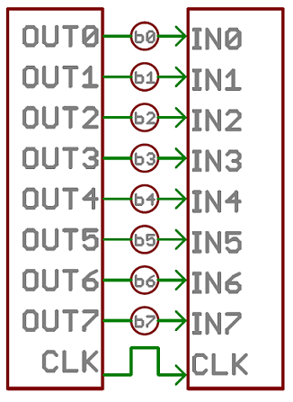
An 8-bit data bus, controlled by a clock, transmitting a byte every clock pulse. 9 wires are used.
Serial interfaces stream their data, one single bit at a time. These
interfaces can operate on as little as one wire, usually never more than
four.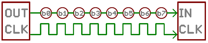
Example of a serial interface, transmitting one bit every clock pulse. Just 2 wires required!
Think of the two interfaces as a stream of cars: a parallel interface
would be the 8+ lane mega-highway, while a serial interface is more
like a two-lane rural country road. Over a set amount of time, the
mega-highway potentially gets more people to their destinations, but
that rural two-laner serves its purpose and costs a fraction of the
funds to build.Parallel communication certainly has its benefits. It’s fast, straightforward, and relatively easy to implement. But it requires many more input/output (I/O) lines. If you’ve ever had to move a project from a basic Arduino Uno to a Mega, you know that the I/O lines on a microprocessor can be precious and few. So, we often opt for serial communication, sacrificing potential speed for pin real estate.
Asynchronous Serial
Over the years, dozens of serial protocols have been crafted to meet particular needs of embedded systems. USB (universal serial bus), and Ethernet, are a couple of the more well-known computing serial interfaces. Other very common serial interfaces include SPI, I2C, and the serial standard we’re here to talk about today. Each of these serial interfaces can be sorted into one of two groups: synchronous or asynchronous.A synchronous serial interface always pairs its data line(s) with a clock signal, so all devices on a synchronous serial bus share a common clock. This makes for a more straightforward, often faster serial transfer, but it also requires at least one extra wire between communicating devices. Examples of synchronous interfaces include SPI, and I2C.
Asynchronous means that data is transferred without support from an external clock signal. This transmission method is perfect for minimizing the required wires and I/O pins, but it does mean we need to put some extra effort into reliably transferring and receiving data. The serial protocol we’ll be discussing in this tutorial is the most common form of asynchronous transfers. It is so common, in fact, that when most folks say “serial” they’re talking about this protocol (something you’ll probably notice throughout this tutorial).
The clock-less serial protocol we’ll be discussing in this tutorial is widely used in embedded electronics. If you’re looking to add a GPS module, Bluetooth, XBee’s, serial LCDs, or many other external devices to your project, you’ll probably need to whip out some serial-fu.
Suggested Reading
This tutorial builds on a few lower-level electronics concepts, including:- How to read a schematic
- Analog vs Digital
- Logic Levels
- Binary
- Hexadecimal
- ASCII
Now then, let’s go on a serial journey…
Rules of Serial
The asynchronous serial protocol has a number of built-in rules - mechanisms that help ensure robust and error-free data transfers. These mechanisms, which we get for eschewing the external clock signal, are:- Data bits,
- Synchronization bits,
- Parity bits,
- and Baud rate.
Baud Rate
The baud rate specifies how fast data is sent over a serial line. It’s usually expressed in units of bits-per-second (bps). If you invert the baud rate, you can find out just how long it takes to transmit a single bit. This value determines how long the transmitter holds a serial line high/low or at what period the receiving device samples its line.Baud rates can be just about any value within reason. The only requirement is that both devices operate at the same rate. One of the more common baud rates, especially for simple stuff where speed isn’t critical, is 9600 bps. Other “standard” baud are 1200, 2400, 4800, 19200, 38400, 57600, and 115200.
The higher a baud rate goes, the faster data is sent/received, but there are limits to how fast data can be transferred. You usually won’t see speeds exceeding 115200 - that’s fast for most microcontrollers. Get too high, and you’ll begin to see errors on the receiving end, as clocks and sampling periods just can’t keep up.
Framing the data
Each block (usually a byte) of data transmitted is actually sent in a packet or frame of bits. Frames are created by appending synchronization and parity bits to our data.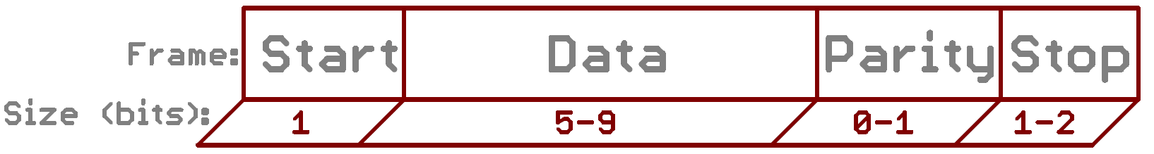
A serial frame. Some symbols in the frame have configurable bit sizes.
Let’s get into the details of each of these frame pieces.Data chunk
The real meat of every serial packet is the data it carries. We ambiguously call this block of data a chunk, because its size isn’t specifically stated. The amount of data in each packet can be set to anything from 5 to 9 bits. Certainly, the standard data size is your basic 8-bit byte, but other sizes have their uses. A 7-bit data chunk can be more efficient than 8, especially if you’re just transferring 7-bit ASCII characters.After agreeing on a character-length, both serial devices also have to agree on the endianness of their data. Is data sent most-significant bit (msb) to least, or vice-versa? If it’s not otherwise stated, you can usually assume that data is transferred least-significant bit (lsb) first.
Synchronization bits
The synchronization bits are two or three special bits transferred with each chunk of data. They are the start bit and the stop bit(s). True to their name, these bits mark the beginning and end of a packet. There’s always only one start bit, but the number of stop bits is configurable to either one or two (though it’s commonly left at one).The start bit is always indicated by an idle data line going from 1 to 0, while the stop bit(s) will transition back to the idle state by holding the line at 1.
Parity bits
Parity is a form of very simple, low-level error checking. It comes in two flavors: odd or even. To produce the parity bit, all 5-9 bits of the data byte are added up, and the evenness of the sum decides whether the bit is set or not. For example, assuming parity is set to even and was being added to a data byte like0b01011101, which has an odd number of 1’s (5), the parity bit would be set to 1. Conversely, if the parity mode was set to odd, the parity bit would be 0.Parity is optional, and not very widely used. It can be helpful for transmitting across noisy mediums, but it’ll also slow down your data transfer a bit and requires both sender and receiver to implement error-handling (usually, received data that fails must be re-sent).
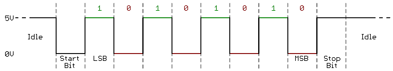
9600 8N1 (an example)
9600 8N1 - 9600 baud, 8 data bits, no parity, and 1 stop bit - is one of the more commonly used serial protocols. So, what would a packet or two of 9600 8N1 data look like? Let’s have an example!A device transmitting the ASCII characters ‘O’ and ‘K’ would have to create two packets of data. The ASCII value of O (that’s uppercase) is 79, which breaks down into an 8-bit binary value of
01001111, while K’s binary value is 01001011. All that’s left is appending sync bits.It isn’t specifically stated, but it’s assumed that data is transferred least-significant bit first. Notice how each of the two bytes is sent as it reads from right-to-left.
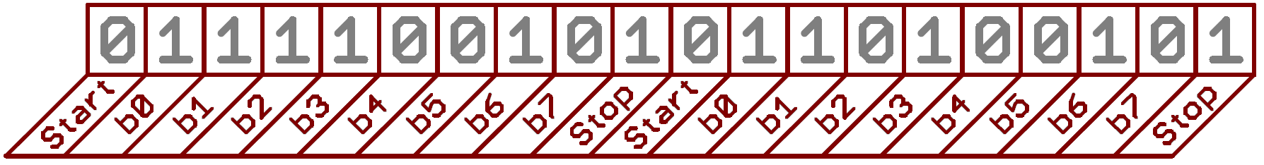
For every byte of data transmitted, there are actually 10 bits being sent: a start bit, 8 data bits, and a stop bit. So, at 9600 bps, we’re actually sending 9600 bits per second or 960 (9600/10) bytes per second.
Now that you know how to construct serial packets, we can move on to the hardware section. There we’ll see how those 1’s and 0’s and the baud rate are implemented at a signal level!
Wiring and Hardware
A serial bus consists of just two wires - one for sending data and another for receiving. As such, serial devices should have two serial pins: the receiver, RX, and the transmitter, TX.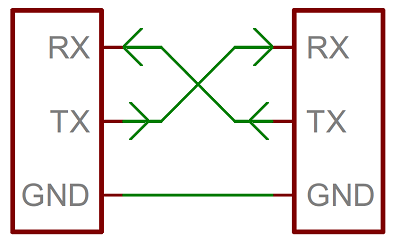
A serial interface where both devices may send and receive data is either full-duplex or half-duplex. Full-duplex means both devices can send and receive simultaneously. Half-duplex communication means serial devices must take turns sending and receiving.
Some serial busses might get away with just a single connection between a sending and receiving device. For example, our Serial Enabled LCDs are all ears and don’t really have any data to relay back to the controlling device. This is what’s known as simplex serial communication. All you need is a single wire from the master device’s TX to the listener’s RX line.
Hardware Implementation
We’ve covered asynchronous serial from a conceptual side. We know which wires we need. But how is serial communication actually implemented at a signal level? In a variety ways, actually. There are all sorts of standards for serial signaling. Let’s look at a couple of the more popular hardware implementations of serial: logic-level (TTL) and RS-232.When microcontrollers and other low-level ICs communicate serially they usually do so at a TTL (transistor-transistor logic) level. TTL serial signals exist between a microcontroller’s voltage supply range - usually 0V to 3.3V or 5V. A signal at the VCC level (3.3V, 5V, etc.) indicates either an idle line, a bit of value 1, or a stop bit. A 0V (GND) signal represents either a start bit or a data bit of value 0.
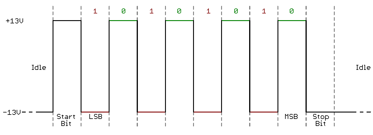
When you’re connecting two serial devices together, it’s important to make sure their signal voltages match up. You can’t directly interface a TTL serial device with an RS-232 bus. You’ll have to shift those signals!
Continuing on, we’ll explore the tool microcontrollers use to convert their data on a parallel bus to and from a serial interface. UARTs!
UARTs
The final piece to this serial puzzle is finding something to both create the serial packets and control those physical hardware lines. Enter the UART.A universal asynchronous receiver/transmitter (UART) is a block of circuitry responsible for implementing serial communication. Essentially, the UART acts as an intermediary between parallel and serial interfaces. On one end of the UART is a bus of eight-or-so data lines (plus some control pins), on the other is the two serial wires - RX and TX.
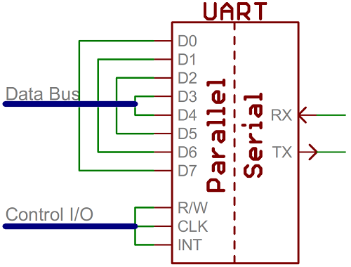
Super-simplified UART interface. Parallel on one end, serial on the other.
UARTs do exist as stand-alone ICs, but they’re more commonly found
inside microcontrollers. You’ll have to check your microcontroller’s
datasheet to see if it has any UARTs. Some have none, some have one,
some have many. For example, the Arduino Uno - based on the “old
faithful” ATmega328 - has just a single UART, while the Arduino Mega -
built on an ATmega2560 - has a whopping four UARTs.As the R and T in the acronym dictate, UARTs are responsible for both sending and receiving serial data. On the transmit side, a UART must create the data packet - appending sync and parity bits - and send that packet out the TX line with precise timing (according to the set baud rate). On the receive end, the UART has to sample the RX line at rates according to the expected baud rate, pick out the sync bits, and spit out the data.
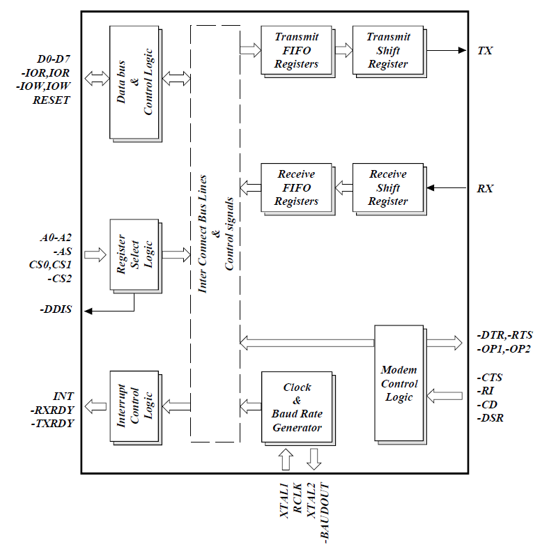
Internal UART block diagram (courtesy of the Exar ST16C550 datasheet)
More advanced UARTs may throw their received data into a buffer,
where it can stay until the microcontroller comes to get it. UARTs will
usually release their buffered data on a first-in-first-out (FIFO)
basis. Buffers can be as small as a few bits, or as large as thousands
of bytes.Software UARTs
If a microcontroller doesn’t have a UART (or doesn’t have enough), the serial interface can be bit-banged - directly controlled by the processor. This is the approach Arduino libraries like SoftwareSerial take. Bit-banging is processor-intensive, and not usually as precise as a UART, but it works in a pinch!Common Pitfalls
That’s about all there is to serial communication. I’d like to leave you with a few common mistakes that are easy for an engineer of any experience level to make:RX-to-TX, TX-to-RX
Seems simple enough, but it’s a mistake I know I’ve made more than a few times. As much as you want their labels to match up, always make sure to cross the RX and TX lines between serial devices.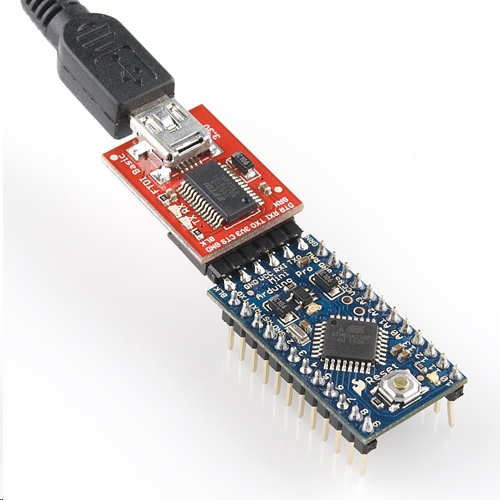
FTDI Basic programming a Pro Mini. Note RX and TX’s crossed!
Contrary to what the esteemed Dr. Egon Spengler would warn, cross the streams.Baud Rate Mismatch
Baud rates are like the languages of serial communication. If two devices aren’t speaking at the same speed, data can be either misinterpreted, or completely missed. If all the receiving device sees on its receive line is garbage, check to make sure the baud rates match up.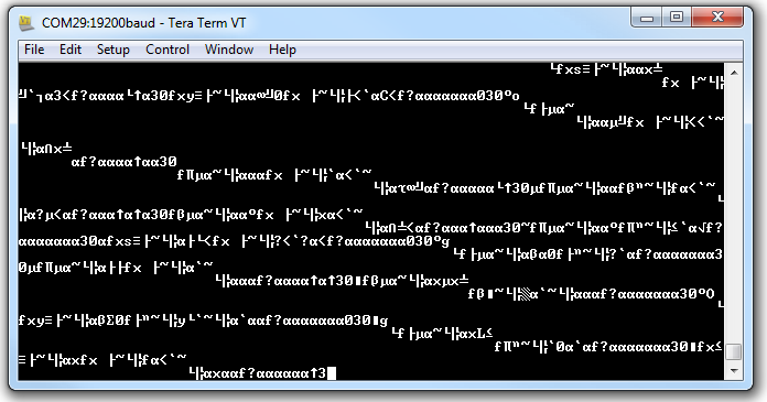
Data transmitted at 9600 bps, but received at 19200 bps. Baud mismatch = garbage.
Bus Contention
Serial communication is designed to allow just two devices to communicate across one serial bus. If more than one device is trying to transmit on the same serial line you could run into bus-contention. Dun dun dun….For example, if you’re connecting a GPS module up to your Arduino, you may just wire that module’s TX line up the Arduino’s RX line. But that Arduino RX pin is already wired up to the TX pin of the USB-to-serial converter, which is used whenever you program the Arduino or use the Serial Monitor. This sets up the potential situation where both the GPS module and FTDI chip are trying to transmit on the same line at the same time.
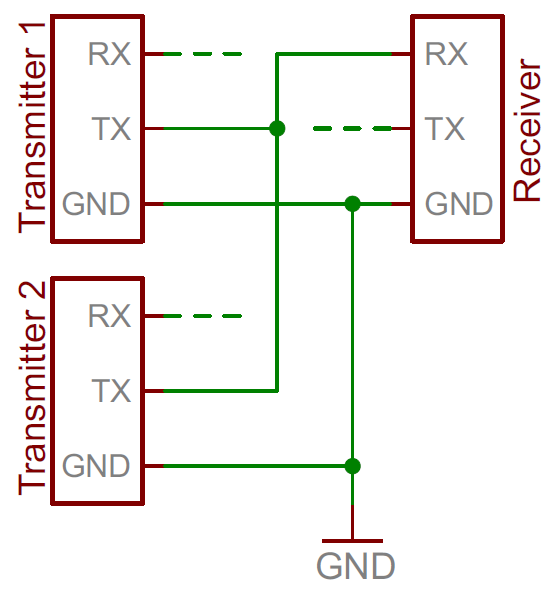
Two transmitters sending to a single receiver sets up the possibility for bus contention.
Two devices trying to transmit data at the same time, on the same
line, is bad! At “best” neither of the devices will get to send their
data. At worst, both device’s transmit lines go poof (though that’s
rare, and usually protected against).It can be safe to connect multiple receiving devices to a single transmitting device. Not really up to spec and probably frowned upon by a hardened engineer, but it’ll work. For example, if you’re connecting a serial LCD up to an Arduino, the easiest approach may be to connect the LCD module’s RX line to the Arduino’s TX line. The Arduino’s TX is already connected to the USB programmer’s RX line, but that still leaves just one device in control of the transmission line.
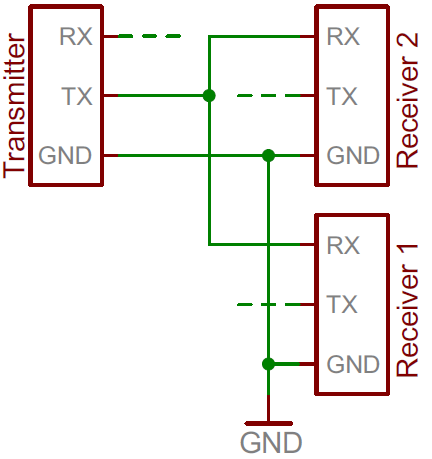
In general - one serial bus, two serial devices!
Serial UART types
Serial communication on PC compatibles started with the 8250 UART in the IBM XT. In the years after, new family members were introduced like the 8250A and 8250B revisions and the 16450. The last one was first implemented in the AT. The higher bus speed in this computer could not be reached by the 8250 series. The differences between these first UART series were rather minor. The most important property changed with each new release was the maximum allowed speed at the processor bus side. The 16450 was capable of handling a communication speed of 38.4 kbs without problems. The demand for higher speeds led to the development of newer series which would be able to release the main processor from some of its tasks. The main problem with the original series was the need to perform a software action for each single byte to transmit or receive. To overcome this problem, the 16550 was released which contained two on-board FIFO buffers, each capable of storing 16 bytes. One buffer for incomming, and one buffer for outgoing bytes.A marvellous idea, but it didn't work out that way. The 16550 chip contained a firmware bug which made it impossible to use the buffers. The 16550A which appeared soon after was the first UART which was able to use its FIFO buffers. This made it possible to increase maximum reliable communication speeds to 115.2 kbs. This speed was necessary to use effectively modems with on-board compression. A further enhancment introduced with the 16550 was the ablity to use DMA, direct memory access for the data transfer. Two pins were redefined for this purpose. DMA transfer is not used with most applications. Only special serial I/O boards with a high number of ports contain sometimes the necessary extra circuitry to make this feature work.
The 16550A is the most common UART at this moment. Newer versions are under development, including the 16650 which contains two 32 byte FIFO's and on board support for software flow control. Texas Instruments is developing the 16750 which contains 64 byte FIFO's.
Registers
Eight I/O bytes are used for each UART to access its registers. The following table shows, where each register can be found. The base address used in the table is the lowest I/O port number assigned. The switch bit DLAB can be found in the line control register LCR as bit 7 at I/O address base + 3.| DLAB = 0 | DLAB = 1 | |||
|---|---|---|---|---|
| I/O port | Read | Write | Read | Write |
| base | RBR receiver buffer | THR transmitter holding | DLL divisor latch LSB | |
| base + 1 | IER interrupt enable | IER interrupt enable | DLM divisor latch MSB | |
| base + 2 | IIR interrupt identification | FCR FIFO control | IIR interrupt identification | FCR FIFO control |
| base + 3 | LCR line control | |||
| base + 4 | MCR modem control | |||
| base + 5 | LSR line status | – factory test | LSR line status | – factory test |
| base + 6 | MSR modem status | – not used | MSR modem status | – not used |
| base + 7 | SCR scratch | |||
- Available registers
- RBR, receiver buffer register
- THR, transmitter holding register
- IER, interrupt enable register
- IIR, interrupt identification register
- FCR, FIFO control register
- LCR, line control register
- MCR, modem control register
- LSR, line status register
- MSR, modem status register
- SCR, scratch register
- DLL, divisor latch LSB
- DLM, divisor latch MSB
RBR : Receiver buffer register (RO)
The RBR, receiver buffer register contains the byte received if no FIFO is used, or the oldest unread byte with FIFO's. If FIFO buffering is used, each new read action of the register will return the next byte, until no more bytes are present. Bit 0 in the LSR line status register can be used to check if all received bytes have been read. This bit wil change to zero if no more bytes are present.THR : Transmitter holding register (WO)
The THR, transmitter holding register is used to buffer outgoing characters. If no FIFO buffering is used, only one character can be stored. Otherwise the amount of characters depends on the type of UART. Bit 5 in the LSR, line status register can be used to check if new information must be written to THR. The value 1 indicates that the register is empty. If FIFO buffering is used, more than one character can be written to the transmitter holding register when the bit signals an empty state. There is no indication of the amount of bytes currently present in the transmitter FIFO. The transmitter holding register is not used to transfer the data directly. The byte is first transferred to a shift register where the information is broken in single bits which are sent one by one.IER : Interrupt enable register (R/W)
The smartest way to perform serial communications on a PC is using interrupt driven routines. In that configuration, it is not necessary to poll the registers of the UART periodically for state changes. The UART will signal each change by generating a processor interrupt. A software routine must be present to handle the interrupt and to check what state change was responsible for it. Interrupts are not generated, unless the UART is told to do so. This is done by setting bits in the IER, interrupt enable register. A bit value 1 indicates, that an interrupt may take place.| Bit | Description |
|---|---|
| 0 | Received data available |
| 1 | Transmitter holding register empty |
| 2 | Receiver line status register change |
| 3 | Modem status register change |
| 4 | Sleep mode (16750 only) |
| 5 | Low power mode (16750 only) |
| 6 | reserved |
| 7 | reserved |
IIR : Interrupt identification register (RO)
A UART is capable of generating a processor interrupt when a state change on the communication device occurs. One interrupt signal is used to call attention. This means, that additional information is needed for the software before the necessary actions can be performed. The IIR, interrupt identification register is helpful in this situation. Its bits show the current state of the UART and which state change caused the interrupt to occur.| Bit | Value | Description | Reset by | |||||
|---|---|---|---|---|---|---|---|---|
| 0 | 0 | Interrupt pending | – | |||||
| 1 | No interrupt pending | – | ||||||
| 1,2,3 | Bit 3 | Bit 2 | Bit 1 | |||||
| 0 | 0 | 0 | Modem status change | MSR read | ||||
| 0 | 0 | 1 | Transmitter holding register empty | IIR read or THR write | ||||
| 0 | 1 | 0 | Received data available | RBR read | ||||
| 0 | 1 | 1 | Line status change | LSR read | ||||
| 1 | 1 | 0 | Character timeout (16550) | RBR read | ||||
| 4 | 0 | Reserved | – | |||||
| 5 | 0 | Reserved (8250, 16450, 16550) | – | |||||
| 1 | 64 byte FIFO enabled (16750) | – | ||||||
| 6,7 | Bit 7 | Bit 6 | ||||||
| 0 | 0 | No FIFO | – | |||||
| 1 | 0 | Unusable FIFO (16550 only) | – | |||||
| 1 | 1 | FIFO enabled | – | |||||
FCR : FIFO control register (WO)
The FCR, FIFO control register is present starting with the 16550 series. This register controls the behaviour of the FIFO's in the UART. If a logical value 1 is written to bits 1 or 2, the function attached is triggered. The other bits are used to select a specific FIFO mode.| Bit | Value | Description | |
|---|---|---|---|
| 0 | 0 | Disable FIFO's | |
| 1 | Enable FIFO's | ||
| 1 | 0 | – | |
| 1 | Clear receive FIFO | ||
| 2 | 0 | – | |
| 1 | Clear transmit FIFO | ||
| 3 | 0 | Select DMA mode 0 | |
| 1 | Select DMA mode 1 | ||
| 4 | 0 | Reserved | |
| 5 | 0 | Reserved (8250, 16450, 16550) | |
| 1 | Enable 64 byte FIFO (16750) | ||
| 6,7 | Bit 7 | Bit 6 | Receive FIFO interrupt trigger level |
| 0 | 0 | 1 byte | |
| 0 | 1 | 4 bytes | |
| 1 | 0 | 8 bytes | |
| 1 | 1 | 14 bytes | |
LCR : Line control register (R/W)
The LCR, line control register is used at initialisation to set the communication parameters. Parity and number of data bits can be changed for example. The register also controls the accessibility of the DLL and DLM registers. These registers are mapped to the same I/O port as the RBR, THR and IER registers. Because they are only accessed at initialisation when no communication occurs this register swapping has no influence on performance.| Bit | Value | Description | |||||
|---|---|---|---|---|---|---|---|
| 0,1 | Bit 1 | Bit 0 | Data word length | ||||
| 0 | 0 | 5 bits | |||||
| 0 | 1 | 6 bits | |||||
| 1 | 0 | 7 bits | |||||
| 1 | 1 | 8 bits | |||||
| 2 | 0 | 1 stop bit | |||||
| 1 | 1.5 stop bits (5 bits word) 2 stop bits (6, 7 or 8 bits word) | ||||||
| 3,4,5 | Bit 5 | Bit 4 | Bit 3 | ||||
| x | x | 0 | No parity | ||||
| 0 | 0 | 1 | Odd parity | ||||
| 0 | 1 | 1 | Even parity | ||||
| 1 | 0 | 1 | High parity (stick) | ||||
| 1 | 1 | 1 | Low parity (stick) | ||||
| 6 | 0 | Break signal disabled | |||||
| 1 | Break signal enabled | ||||||
| 7 | 0 | DLAB : RBR, THR and IER accessible | |||||
| 1 | DLAB : DLL and DLM accessible | ||||||
The UART is capable of generating a trailing bit at the end of each dataword which can be used to check some data distortion. Because only one bit is used, the parity system is capable of detecting only an odd number of false bits. If an even number of bits has been flipped, the error will not be seen.
When even parity is selected, the UART assures that the number of high bit values in the sent or received data is always even. Odd parity setting does the opposite. Using stick parity has very little use. It sets the parity bit to always 1, or always 0.
Common settings are:
- 8 data bits, one stop bit, no parity
- 7 data bits, one stop bit, even parity
MCR : Modem control register (R/W)
The MCR, modem control register is used to perform handshaking actions with the attached device. In the original UART series including the 16550, setting and resetting of the control signals must be done by software. The new 16750 is capable of handling flow control automatically, thereby reducing the load on the processor.| Bit | Description |
|---|---|
| 0 | Data terminal ready |
| 1 | Request to send |
| 2 | Auxiliary output 1 |
| 3 | Auxiliary output 2 |
| 4 | Loopback mode |
| 5 | Autoflow control (16750 only) |
| 6 | Reserved |
| 7 | Reserved |
LSR : Line status register (RO)
The LSR, line status register shows the current state of communication. Errors are reflected in this register. The state of the receive and transmit buffers is also available.| Bit | Description |
|---|---|
| 0 | Data available |
| 1 | Overrun error |
| 2 | Parity error |
| 3 | Framing error |
| 4 | Break signal received |
| 5 | THR is empty |
| 6 | THR is empty, and line is idle |
| 7 | Errornous data in FIFO |
MSR : Modem status register (RO)
The MSR, modem status register contains information about the four incomming modem control lines on the device. The information is split in two nibbles. The four most siginificant bits contain information about the current state of the inputs where the least significant bits are used to indicate state changes. The four LSB's are reset, each time the register is read.| Bit | Description |
|---|---|
| 0 | change in Clear to send |
| 1 | change in Data set ready |
| 2 | trailing edge Ring indicator |
| 3 | change in Carrier detect |
| 4 | Clear to send |
| 5 | Data set ready |
| 6 | Ring indicator |
| 7 | Carrier detect |
SCR : Scratch register (R/W)
The SCR, scratch register was not present on the 8250 and 8250B UART. It can be used to store one byte of information. In practice, it has only limited use. The only real use I know of is checking if the UART is a 8250/8250B, or a 8250A/16450 series. Because the 8250 series are only found in XT's even this use of the register is not commonly seen anymore.DLL and DLM : Divisor latch registers (R/W)
For generating its timing information, each UART uses an oscillator generating a frequency of about 1.8432 MHz. This frequency is divided by 16 to generate the time base for communucation. Because of this division, the maximum allowed communication speed is 115200 bps. Modern UARTS like the 16550 are capable of handling higher input frequencies up to 24 MHz which makes it possible to communicate with a maximum speed of 1.5 Mbps. On PC's higher frequencies than the 1.8432 MHz are rarely seen because this would be software incompatible with the original XT configuration.This 115200 bps communication speed is not suitable for all applications. To change the communication speed, the frequency can be further decreased by dividing it by a programmable value. For very slow communications, this value can go beyond 255. Therefore, the divisor is stored in two seperate bytes, the divisor latch registers DLL and DLM which contain the least, and most significant byte.
For error free communication, it is necessary that both the transmitting and receiving UART use the same time base. Default values have been defined which are commonly used. The table shows the most common values with the appropriate settings of the divisor latch bytes. Note that these values only hold for a PC compatible system where a clock frequency of 1.8432 MHz is used.
| Speed (bps) | Divisor | DLL | DLM |
|---|---|---|---|
| 50 | 2,304 | 0x00 | 0x09 |
| 300 | 384 | 0x80 | 0x01 |
| 1,200 | 96 | 0x60 | 0x00 |
| 2,400 | 48 | 0x30 | 0x00 |
| 4,800 | 24 | 0x18 | 0x00 |
| 9,600 | 12 | 0x0C | 0x00 |
| 19,200 | 6 | 0x06 | 0x00 |
| 38,400 | 3 | 0x03 | 0x00 |
| 57,600 | 2 | 0x02 | 0x00 |
| 115,200 | 1 | 0x01 | 0x00 |

No comments:
Post a Comment